한국산학기술학회논문지 Vol. 10, No. 2, pp. 248-255, 2009
Max-based Analog Absolute Circuits with Small Error
Maheshwar pd.sah1, Hai-ping Lin1, Changju Yang1, Junho Lee2, Hyongsuk Kim1*
Abstract
Error is the major problem in communication system. Absolute circuit is one of the most important building blocks to implement for the error measurement in communication system as well as in analog circuit design. The main goal of this paper is to design a circuit with high accuracy and minimum error performance. In this paper, a new current mode absolute circuit is implemented to calculate the absolute value of two signals. This new design shows enhanced performance and low distortion over the previous implementation. The proposed circuit is simulated using Hspice and implemented in analog viterbi decoder. It is very suitable for implementing in error calculation for the large scale integrated circuit. Hspice simulation results of previous and new one circuit are reported. Key Words : current mode, Analog absolute circuit, max-based, small error.
작은 에러를 갖는 Max 회로 기반 아날로그 절대값 계산 회로 마헤스워 사 1 , 임해평 1 , 양창주 1 , 이준호 2 , 김형석 1*
요 약 통신시스템에서의 에러의 처리는 매우 중요한 문제로서 비터비 디코더와 같은 에러처리를 위해서 주로 절 대값으로 표현하기 때문에 아날로그 절대값 회로가 자주 필요하게 된다 . 이 논문에서는 절대값을 정확하게 계산할 수 있는 아날로그 절대값 회로를 제안하였다 . 제안한 절대값 회로에는 부호가 반대인 두 신호들을 만든 다음 , 이 신 호들을 아날로그 MAX 회로에 인가하여 둘 중 최대값을 출력하게 하는 방법이다 . 이 구조를 회로로 구현하기 위해서 는 두 개의 입력 신호를 반대방향으로 차를 구하여 , 크기는 같고 부호가 다른 두 개의 신호를 만든 다음 이들을 MAX 회로의 입력으로 사용하는 회로를 설계하였다 . 본 논문에서는 제안한 회로를 Hspice 를 이용하여 시뮬레이션을 수행했으며 , 그 결과를 제시하였다 .
1. INTRODUCTION
2. ANALOG ABSOLUTE CIRCUITS
I ref 1 = 1 2 μ n C ox ( W / L ) 1 ( V GS − V T ) 2 (1 + λ V DS 1 ) (1) Similarly for Mn2, I out 1 = 1 2 μ n C ox ( W L ) 2 ( V GS − V T ) 2 (1 + λ V DS 2 ) (2)
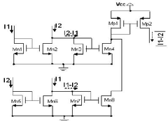
[Fig. 1] Simple two subtraction absolute circuit.
Generally channel Length modulation λ is zero I out 1 = ( W / L ) 2 I ref 1 ( W / L ) 1 (3) The output across Mn4 is given by I out = ( ( W W Mn Mn 4 3 L L Mn Mn 3 4 ) ) ⎢ ⎣ ⎡ I 2 − ( W ( W Mn Mn 2 1 L L Mn Mn 2 1 ) ) I 1 ⎦ ⎥ ⎤ for I 2 > I 1
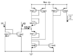
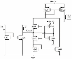
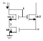
= 0 for I 2 ≤ I 1 (4) If the aspects ratios (W/L) of upper and lower are same I out = I 2 − I 1 for I 2 > I 1 = 0 for I 1 ≤ I 2 (5) Similarly for the lower part of the circuit, the current at Mn8 is, = 0 for I 1 ≤ I 2 (6) When I 1 > I 2 , the drain voltage of Mn2 drops quickly so that Mn4 becomes cut off. Meanwhile, the current (I 1 -I 2 ) obtained at the lower part of the circuit is fed into the diode connected circuit of Mn7. In the end, the current mirror Mn8 produces I 1 -I 2 . The current is copied by another current mirror Mp1 and Mp2. When I 2 >I 1 , Mn8 is cut off and I 2 -I 1 obtained from the upper part of the circuit. The major drawback of this approach is at the zero crossing of the two input currents or when I 1 =I 2 . The current at the drain terminal of Mn2 and Mn6 become zero. Therefore, the voltage at this point is also zero. In this moment Vd<Vg>Vs which shows the MOSFET temporarily in the triode region instead of cut off mode. So the circuit creates maximum error compare to the ideal output of absolute current (I 1 -I 2 ). The circuit can not operate at high frequency mode due to high output impedance. Another solution for increasing the performance at the zero crossing of the current signal is a simple full wave current rectifier. circuit with diode connected MOSFETS as shown in Fig. 2. Here Mp1 and Mn3 are equivalent of two diodes connected with opposite polarity. When (I 2 -I 1 ) >0, Mp1 will forward bias and current flows across Mn4 which is copied to Mn5. The operation is reversed when (I 2 -I 1 ) <0, Mn3 will forward bias and current flows across Mp2 to Mp3. Therefore, the total output across Mp5 is absolute value of (I 1 -I 2 ). The performance of the real output is better than previous circuit and nearly same as ideal. One of the problems associated in this circuit is the inherent error after completion of one cycle. In each cycle of operation either Mn3 or Mp2 should be cut off while other is in saturation but temporally one MOS is always in triode region which tends to maximum error and feed back highly distortion in the input signal. The distortion in the input signal can be modified using a simple comparator circuit [9- 10]. It is based on subtraction (Mn1, Mn2) and comparator (Mn3, Mp1, Mp2, Mn4) as shown in Fig. 3. It has input impedance rPMOS//rNMOS. The input state of this architecture has source follower which introduces feed back into the gates. A positive feedback from an inverter is used to achieve enough gain to amplify small voltage variation in the input stage node [15]. When (I 2 -I 1 )>0 or I 2 >I 1 , the source follower of Mp1 and Mn3 are forward and reverse bias respectively. Simultaneously the inverter of Mn4 turns on, so the drain voltage of this MOS will low. The feedback across the drain of Mn4 turns on the MOS Mp1 and (I 2 -I 1 ) obtained across Mn5. The current is copied by current mirror Mn6. The situation is reversed when (I 2 -I 1 ) <0 or (I 2 <I 1 ), Mn3 will forward bias and the inverter of Mp2 turns on. The drain voltage of this MOS is high, so the feedback of the inverter turns on Mn3 and (I 1 -I 2 ) is obtained across Mp3 to Mp4. Therefore, the total output current across Mp4 is absolute value of (I 1 -I 2 ). The circuit however shows deadband region for dynamic response of small input current in which the two input transistors are turned off temporarily [16]. At this time the input resistance is quite high and thus limiting the speed of operation and some delay between the real and ideal output of the current signal [18]. In this paper, a new CMOS current absolute circuit is proposed which takes advantages such as simple structure, low power consumption and low distortion compared to above circuits. Hspice is used to verify the simulation result of the circuit.I out = I 1 − I 2 for I 1 > I 2[Fig. 2] Current rectification based absolute Circuit.[Fig. 3] Comparator based absolute circuit.[Fig. 4] Basic cell of max circuit.[Fig. 5] Proposed max based absolute circuit.
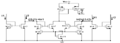
3. PROPOSED CIRCUIT
4. SIMULATION RESULTS
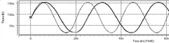
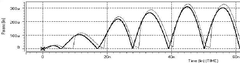
[Fig. 6] Input waveform.
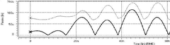
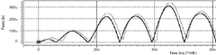
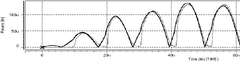
substractor and max circuit result a time delay between real and ideal output. The average error of 1.40% between real and ideal output confirms an excellent progress of the circuit. The power dissipation, speed of operation and power delay product are too optimistic as subtraction circuit also consumes certain amount of power and exhibits certain delay time [18]. So all the circuits present in this paper show little bit delay with real and ideal output as absolute circuits consist subtraction of current signal. The comparison results of the circuits are summarized in Table 2.
5. CONCLUSION
(a)
(b)
(c)
(d) real output ideal output [Fig. 7] Output waveform of the absolute circuits: (a) Two subtraction based (b) Current rectifier based (c) Comparator based (d) Max based.
[Table 2] Comparison results Time delay S.n Circuits (n sec) 1 Two Subtraction absolute circuit 1.2 Full wave rectification based absolute 2 1.4 circuit 3 Comparator based absolute circuit 1.5 4 Max based absolute circuit 1.5
REFERENCES
- [1] Aly M. Ismail and Ahmed M. soliman, "Novel CMOS voltage mode absolute value circuit," International journal of electronics and Communication, vol. 53, no. 2, pp.114-116, Urban and fischer Verlag, Nov. 10, 1998.
- [2] Zhenhua Wang, "Current–mode integrated circuits for analog computation and signal processing,"on analog integrated circuits and signal processing- 1, pp. 287-295, Kluwer academic publisher Nether land, June 18, 1991.
- [3] C. S Hilas and Th. Lapoulos, "A study of voltage mode to current mode conversion techniques," in proc of IEEE conf, on circuit design, pp. 1309-1312, 1996.
- [4] Chuen Yan Chen, Chun-Yurh Huang, Ju-Ying Tsao and Bin-Da Liu, "A current mode circuit for Euclidian distant calculation,"in proc. of IEEE conf. on VLSI technology system and application on technical paper internal symposium, pp. 83-86, Jun 3, 1997.
- [5] Bogdan M. Wilmowski, Mahmut Ersin Sinangi and Gunhan Dundar, "A gray-code current mode ADC Structure," in proc. of, IEEE conf. on circuit and systems, pp. 35-38, Benalmadena (Malaga), Spain, May 2006.
- [6] Hyongsuk Kim, Hongrak Son, Tamás Roska and Leon O. Chua, "Very high speed viterbi decoder with circularly connected analog CNN cell array," in proc. of IEEE ISCAS conf. on circuit and system, pp. 97-100, May.
- [7] Hyongsuk Kim, Hongak Son, Tamas Roska and Leon O Chua, "High performance viterbi decoder with circularly connected 2-D CNN unilateral cell array," IEEE Trans. on circuit and systems -1, vol. 52, no. 10, pp. 2208-2218, Oct. 2005. .
- [8] Hyunjung Kim, Hongrak Son, Jeonwon Lee, In-cheon Kim and Hyongsuk Kim, "Analog viterbi decoder for PRML using analog Parallel processing circuits of the CNN," in proc of IEEE conf. on cellular neural networks and their application, Istanbul, Turkey, August 2006.
- [9] S. Vlassis and S. Siskos, "Precision multi –input current comparator and it’s application to analog median filter implementation," of analog integrated circuits and signal processing, vol. 34, pp. 233-245, Kluwer academic publisher Netherland, July 2002.
- [10] Chartchai Noisuwan, Jintan Nakasuwan, Boonying knobnob, Sonar Chivapreecha and Kobchai Dejhan, "A CMOS median filter circuit design,"in proc. of IEEE ISCIT conf. on circuit and system pp. 1089-1092, Bangkok Thailand, Oct.2006.
- [11] I. Baturone, J.L,Huertas, A.Barriga and S.sanchez Solano, "Current mode multiple input max circuit ,"Electron. Lett. vol. 30, no. 9, pp. 678-680, April 28, 1994.
- [12] I.Baturone, A.Barriga, J.L.Huertas, "Multi-input voltage and current mode min/max circuits," 3rd International conference on fuzzy logic, neural networks and soft computing, pp. 649-650, Japan, Aug. 1994.
- [13] C.Y Huang and B.D.Liu, "Current mode multiple input maximum circuit for fuzzy logic controllers," Electron. Lett. vol. 30, no. 23, pp. 1924-1925, Nov. 10, 1994.
- [14] L.Ravezzi, D.stoppa and G. F. dalla Betta, "Simple high speed CMOS current comparator," Electron. Lett, vol. 33, no. 2, pp.1829-1830, Oct. 1997.
- [15] Lu Chen, Bingxue and Shi, Chun Lu, "A robust high speed and low Power CMOS current comparator circuit," in proc. of IEEE Asia-pacific conf. on Circuit and system, pp. 174-177, Dec.2000.
- [16] Surachel khucharo ensinand, Varakorn Kasemsuwan, "A 3V robust high speed low input impedance CMOS current comparator,"in proc of IEEE Asia-pacific conference on circuit and system, Dec. 2004.
- [17] Alexandru A. Ciubotaru, "Absolute-value circuit using junction fieldeffect transistors," IEEE Trans. circuits and systems-II, for analog and digital signal processing vol. 50, no. 8, pp. 481-484, Aug. 2003.
- [18] Varakorn Kasemsuwan and Surachet Khucharoensin, "High-speed low input impedance CMOS current comparator," IEEE Trans. on circuit and system,vol. E88-A, no. 6, June 2005.