유기 강유전 박막의 종이기판 응용가능성 검토
AFM, ferroelectric, polarization, P(VDF-TrFE), SEM
Abstract
In this study, It has been demonstrated a new and realizable possibility of the ferroelectric random access memory devices by all solution processing method with paper substrates. Organic ferroelectric poly(vinylidene fluoride-trifluoroethylene) (P(VDF-TrFE)) thin films were formed on paper substrate with Al electrode for the bottom gate structure using spin-coating technique. Then, they were subjected to annealing process for crystallization. The fabricated PVDF-TrFE thin films were observed by scanning electron microscopy (SEM) and atomic force microscopy (AFM). It was found from polarization versus electric field (P-E) measurement that a PVDF-TrFE thin film on paper substrate showed very good ferroelectric property. This result agree well with that of a PVDF-TrFE thin film fabricated on the rigid Si substrate. It anticipated that these results will lead to the emergence of printable electron devices on paper. Furthermore, it could be fabricated by a solution processing method for ferroelectric random access memory device, which is reliable and very inexpensive, has a high density, and can be also fabricated easily.
Journal of the Korea Academia-Industrial http://dx.doi.org/10.5762/KAIS.2015.16.3.2131 cooperation Society ISSN 1975-4701 / eISSN 2288-4688 Vol. 16, No. 3 pp. 2131-2134, 2015
박병은 1* 1 서울시립대학교 전자전기컴퓨터공학부 Experimental study on the Organic Ferroelectric Thin Film on Paper Substrate Byung-Eun Park 1* 1 School of Electrical and Computer Engineering, University of Seoul 요 약 본 논문에서는 종이를 기판으로 사용하고 용액공정이 가능한 강유전체 메모리 소자의 제작 가능성을 검토하였다. 유기물 강유전체인 “폴리비닐리덴트리플루오르에틸렌” 용액을 하부전극이 형성된 종이기판 위에 스핀코핑 방법을 이용하여 도포하였다. 하부전극으로는 진공증착법을 이용하여 알루미늄을 증착하였고, 도포된 “폴리비닐리덴트리플루오르에틸렌” 용 액은 열처리 과정을 통해 결정화하였다. 제작된 “폴리비닐리덴트리플루오르에틸렌” 박막은 주사 전자 현미경법(SEM), 원자 간력 현미경(AFM)을 이용하여 박막의 단면 및 표면의 특성을 평가하였다. 전압에 따른 분극특성 측정을 통해, 종이기판 위 에 형성된 “폴리비닐리덴트리플루오르에틸렌” 박막이 매우 훌륭한 강유전체 특성을 보여주고 있음을 확인하였다. 또한, 종이 기판의 응용가능성을 검토하기 위하여, 실리콘 기판위에 제작한 “폴리비닐리덴트리플루오르에틸렌” 박막과의 비교에 있어서 도 손색없는 강유전체 특성을 보여주고 있음을 알 수 있었다. 이러한 결과들은 종이를 기판으로 이용하여 전자소자들을 제작 할 수 있음을 시사하며, 또한 용액공정으로 고밀도의 저렴한 강유전체 메모리 소자를 손쉽게 제작 할 수 있다는 것을 의미한다.
Key Words :
1. 서론
2131
한국산학기술학회논문지 제16권 제3호, 2015
3. 결론
2. 본론
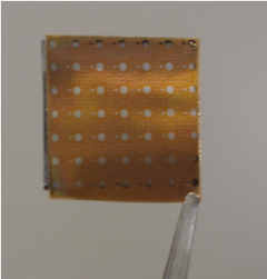
Photograph of a fabricated PVDF-TrFE thin film with upper electrodes on paper substrate.
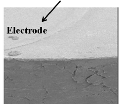
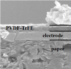
진공증착법을 이용하여 종이기판 위에 하부전극 알루 Fig. 2은 종이기판 위에 제작된 PVDF-TrFE 박막의 미늄을 증착하였다. 하부전극이 형성된 종이기판 위에 주사 전자 현미경 사진이다. Fig. 2(a) 의 경우, 화살표로 졸-겔 (sol-gel) 방법을 이용하여 PVDF-TrFE 용액을 표시된 부분은 상부전극이며, 전체적인 시편의 형태를 도포하였다. PVDF-TrFE 용액은 메틸에틸케톤 (MEK 파악 할 수 있었다. Fig. 2(b)는 제작된 PVDF-TrFE 박 (Methyl Ethyl Ketone))을 용매로 사용하였고, 박막 두께 막의 단면사진이다. 조절을 위해 몰비를 조절하였다. 졸-겔 (sol-gel) 방법을 그림에서 알 수 있듯이 종이기판 위에 형성된 하부전 이용한 전형적인 박막 형성 조건은 3,000rpm, 25초 동안 극 및 용액공정으로 형성된 PVDF-TrFE 박막의 형태를 스핀코팅(spin coating)하였고, 결정화 공정으로 140°C, 명확히 파악 할 수 있었다. 이는 매우 중요한 사항으로 대기상태에서에서 1시간 동안 열처리를 하였다. 전기적 종이를 기판으로 사용하여 박막을 형성하는 경우, 일반 2132
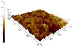
유기 강유전 박막의 종이기판 응용가능성 검토 적으로 종이의 성질상 액체 상태인 용액을 흡수하기 때 Fig. 3은 Fig. 2은 종이기판 위에 제작된 PVDF-TrFE 문에 박막 형성이 불가능하거나 설사 박막이 형성 되었 박막의 원자간력 현미경 사진이다. 을지라도 그 계면상태가 매우 불규칙하거나 단차가 형성 시료는 1μm x 1μm 범위에서 측정되었고, 평균 거칠 되어진다. 그러나 그림에서도 알 수 있듯이 본 실험에서 기 (roughness)는 4.49nm로 매우 평탄한 PVDF-TrFE 제작된 PVDF-TrFE 박막의 경우, 종이를 기판으로 사용 박막이 형성되어 있음을 확인 할 수 있었다. 이러한 결과 했음에도 불구하고 PVDF-TrFE 박막이 균일하게 매우 는 Fig. 2에서도 알 수 있듯이 종이기판 위에 형성된 하 잘 형성되어 있음을 확인 할 수 있었다. 부전극 및 PVDF-TrFE 박막의 매우 뛰어난 계면상태에 기인한다고 생각되어진다.(a)
(b) [Fig. 2] SEM images of a fabricated PVDF-TrFE thin thin film on paper substrate.
[Fig. 4]
[Fig. 3] AFM image of a fabricated PVDF-TrFE thin thin film on paper substrate.
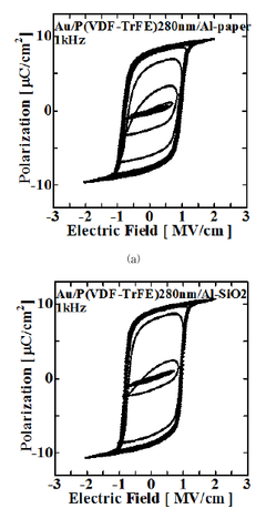
Fig. 4는 전압에 따른 분극특성을 측정한 것이며, 측정 주파수는 1 kHz에서 이루어졌다. Fig. 4 (a) 의 경우, 종 이기판 위에 제작된 PVDF-TrFE 박막의 전압에 따른 분극특성을 측정한 것으로, 잔류분극 값 (Pr : remanent polarization)은 8.3 μC/cm 2 이며, 항전계 값 (Ec : coercive field)은 1.8 MV/cm 이다. Fig. 4(b)는 종이기판 위에 제 작된 PVDF-TrFE 박막과의 분극특성을 비교하기 위하
(b) Polarization versus electric field characteristic of (a) Au/PVDF-TrFE/Al/paper structure (b) Au/PVDF-TrFE/Al/SiO 2 /Si structure
2133
한국산학기술학회논문지 제16권 제3호, 2015 [8]
- T. J. Reece, S. Ducharme, A. V. Sorokin, M Poulsen, "Nonvolatile memory element based on a ferroelectric polymer Langmuir–Blodgett film", Appl. Phys. Lett., 82, pp. 142-144. 2003. DOI: http://dx.doi.org/10.1063/1.1533844 [DOI]
- R. C. G. Naber, M. Bird, H. Sirringhaus, "A gate dielectric that enables high ambipolar mobilities in polymer light-emitting field-effect transistors", Appl. Phys. Lett., 93, 023301. 2008. DOI: http://dx.doi.org/10.1063/1.2957472 [DOI]
- G. H. Gelinck, A. W. Marsman, F. J. Touwslager, S. Setayesh, D. M. de Leeuw, R. C.G Naber, P.W.M Blom, "All-polymer ferroelectric transistors", Appl. Phys. Lett., 87, 092903. 2005. DOI: http://dx.doi.org/10.1063/1.2035324 [11] J Li, D. Taguchi, W. O. Yang, T Manaka, M. Iwamoto, "Interaction of interfacial charge and ferroelectric polarization [DOI]
- C. D. Dimitrakopoulos, P. R.L Malenfantols, “Organic in a pentacene/ poly(vinylidene fluoride-trifluoroethylene) Thin Film Transistors for Large Area Electronics“, Adv. double -layer device", Appl. Phys. Lett., 99, 063302. 2011. [possible DOI]
- Mater., 14, pp. 99-117. 2002. DOI: http://dx.doi.org/10.1063/1.3624477 [possible DOI]
- DOI: 10.1002/1521-4095(20020116)14:2<99::A ID-ADM A99>3.0.CO;2-9 [12] J-W Yoon, B-E Park, H Ishiwara, "Comparative Study [possible DOI]
- H. Sirrinhaus, T. Kawas, R. H. Friend, T. Shimoda, M. on Metal–Ferroelectric–Insulator–Semiconductor Diodes [possible DOI] [alternative DOI]
- Inbasekaran, W. Wu, E. P. Woo, "High-Resolution Inkjet Composed of Poly(vinyliden fluoride-trifluoroethylene) Printing of All-Polymer Transistor Circuits", Science, and Poly(methyl metacrylate)-Blended Poly(vinyliden 290. pp. 2123-2126. 2000. fluoride-trifluoroethylene)", Jpn. J. Appl. Phys., 48, 09KA21, [DOI]
- DOI: DOI: 10.1126/science.290.5499.2123 2009. [possible DOI]
- M. Shtein, J. Mapel, J. B. Benziger, S. R. Forrest, DOI: http://dx.doi.org/10.1143/JJAP.48.09KA21 [DOI]
- "Effects of film morphology and gate dielectric surface preparation on the electrical characteristics of organic-vapor-phase- deposited pentacene thin-film 박 병 은 (Byung-Eun Park) [정회원] [possible DOI]
- transistors", Appl. Phys. Lett., 81, 268-270. 2002. [DOI]
- DOI: http://dx.doi.org/10.1063/1.1491009 • 1999년 3월 : 동경공업대학(공학박 [possible DOI]
- T. Furukawa, "Ferroelectric properties of vinylidene 사) fluoride copolymers", Phase Transition, 18. pp.143-211. 1989. • 1999년 12월 ∼ 2003년 3월 : 동경 [DOI]
- J-H Kim, B-E Park, H. Ishiwara, "Fabrication and 공업대학 조교수 [DOI]
- Electrical Characteristics of M etal– Ferroelectrc– Sem iconductorField • 2011년 4월 ∼ 현재 : 서울시립대 학교 전자전기컴퓨터공학부 교수 [possible DOI]
- Effect Transistor Based on Poly(vinylidene fluoride)", Jpn. J. Appl. Phys., 47, pp. 8472-8475. 2008. [possible DOI]
- DOI: http://dx.doi.org/10.1143/JJAP.47.8472 [possible DOI]
- J-H Kim, B-E Park, "Metal-Ferroelectric- Semiconductor <관심분야> [DOI]
- Field Effect Transistor (MFS-FET) for 1T-type FRAM 반도체 소자, 반도체 재료, 디스플레이 소자, 센서 Based on Polyvinylidene Fluoride (PV DF) Thin Film ", Ferroelectrics, 379, pp. 22-29. 2009. http://dx.doi.org/10.1080/00150190902847893 [DOI]
- G-G Lee, H-S Han, Y-S Choi, B-E Park, "Electrical properties of metal-ferroelectric- insulator-semiconductor field effect transistors (MFIS-FETs) using the polyvinylidene fluoride-trifluoroethylene (P(VDF-TrFE))/ZrO 2 /Si structure", J. Ceram. Soc. Jpn., 118 pp. 1013-1016. 2010. [DOI]
[9]
[10]
여, 같은 박막 조건하에서 실리콘 기판위에 제작한 PVDF-TrFE 박막의 전압에 따른 분극특성을 측정한 것 이다. 측정된 잔류분극 값은 9.2 μC/cm 2 이며, 항전계 값 은 1.8 MV/cm 이다. Fig. 4의 결과에서 알 수 있듯이 종 이를 기판으로 사용한 경우나 기존의 실리콘을 기판으로 사용한 경우나 항전계값은 변화가 없었다. 단지, 종이를 기판으로 사용하여 제작한 PVDF-TrFE 박막의 잔류분 극 값이 다소 적게 나온 것을 확인 할 수 있었다. 이러한 결과들은 종이를 기판으로 사용했음에도 불구하고 제작 된 PVDF-TrFE 박막이 매우 훌륭한 강유전체 특성을 나타내고 있음을 말해준다.
References
[1]
[2]
[3]
[4]
[5]
[6]
[7]
2134